2021-06-15
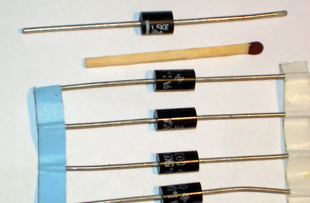
Transient Voltage Suppressor (Transient Voltage Suppressor diode) is also TVS transient suppressor diode, referred to as TVS, is a diode form of high performance protection device. When the poles of the TVS diode are subjected to reverse transient high energy impact, it can change the high impedance between the poles into low impedance at a speed of 10 to the minus 12 seconds, absorbing up to several kilowatts of surge power, so that the voltage clamp between the poles is located at a predetermined value, effectively protecting the precision components in the electronic circuit from damage by various surge pulses. Today, Li Yang Semiconductor and you talk about the characteristics of transient suppression diodes and TVS characteristics and main parameters.
First, the transient suppression diode has the following three characteristics:
1, the TVS diode added to the signal and power line, can prevent the microprocessor or single-chip microcomputer due to instantaneous impulse, such as electrostatic discharge effect, AC power surge and switching power supply noise caused by failure.
2, electrostatic discharge effect can release more than 10000V, more than 60A pulse, and can last 10ms; The general TTL device, when encountered more than 30ms of 10V pulse, will lead to damage. With TVS diodes, the pulse that can cause device damage can be effectively absorbed and interference caused by switching between buses can be eliminated (Crosstalk).
3, the TVS diode is placed in the signal line and ground, can avoid the data and control bus by unnecessary noise.

Second, the characteristics and main parameters of TVS transient suppression diode
1. Characteristic curve of TVS
The circuit symbol of TVS is the same as that of ordinary voltage regulator diodes. Its forward characteristic is the same as that of ordinary diode; The reverse characteristics are typical of PN junction avalanche devices.
Under the action of transient peak pulse current, when the current flowing through TVS rises from the original reverse leakage current ID to IR, the voltage presented at the two poles rises from the rated reverse turn-off voltage VWM to the breakdown voltage VBR, TVS is broken down. With the appearance of peak pulse current, the current flowing through TVS reaches the peak pulse current IPP. The voltage at its poles is clamped below a predetermined maximum clamping voltage. Then, with the exponential attenuation of the pulse current, the voltage at the poles of TVS also continues to decline, and finally returns to the starting state. This is the whole process of TVS inhibiting possible surge pulse power and protecting electronic components.
2, TVS characteristic parameters
1), maximum reverse leakage current ID and rated reverse turn-off voltage VWM. VWM is the maximum continuous DC or pulse voltage of TVS. When this reverse voltage is added to the poles of TVS, it is in a reverse off state, and the current flowing through it should be equal to or equal to its maximum reverse leakage current ID.
2), the most breakdown voltage VBR and breakdown current IR
VBR is the highest avalanche voltage on TVS. At 25℃, TVS is not on before this voltage. When TVS flows through the specified 1mA current (IR), the voltage between the poles of TVS is the most disruptive voltage VBR. According to the dispersion degree of TVS VBR and standard value, TVS can be divided into two kinds: ±5%VBR peaceful coexistence ±10%VBR. For ±5%VBR, VWM=0.85VBR; For ±10%VBR, VWM=0.VBR.

3), maximum clamping voltage VC and maximum peak pulse current IPP
When the pulse peak current IPP with a duration of 20 microseconds flows through TVS, the maximum peak voltage between the two poles is VC. It is a combination of a voltage rise on the series resistance and a temperature coefficient. VC and IPP reflect the surge suppression capability of TVS devices. The ratio of VC to VBR is called the clamping factor and is generally between 1.2 and 1.4.
4), electrical capacity C
The capacitance C is determined by the avalanche junction section of TVS and measured at a specific frequency of 1MHZ. C is proportional to the current bearing capacity of TVS, and too much C will attenuate the signal. Therefore, C is an important parameter for TVS in data interface circuits.
5), maximum peak pulse power consumption PM
PM is the maximum peak pulse dissipation power that TVS can withstand. For the specified test pulse waveform and PM values of various TVS, please refer to the relevant product manual. Under the given maximum clamping voltage, the larger the power dissipation PM, the greater the surge current endurance. Under a given power consumption PM, the lower the clamping voltage VC, the greater the inrush current tolerance. In addition, the peak pulse power consumption is also related to the pulse waveform, duration and ambient temperature. And TVS can withstand the transient pulse is not repeated, the device specified pulse repetition frequency (duration and intermittent time ratio) is 0.01%, if repeated pulse in the circuit, should consider the "accumulation" of pulse power, may cause TVS damage.
6) Clamping time TC
TC is the time from zero to the maximum breakdown voltage VBR. Unipolar TVS for 1×10-12 seconds; For bipolar TVS, at 1 x 10-11 seconds.
Transient suppression diode has been widely used in computer system, communication equipment, AC/DC power supply, automobile, electronic ballast, household appliances, contactor noise suppression and other fields because of its advantages of fast response time, large transient power, low leakage current, breakdown voltage deviation, easy control of clamp voltage, no damage limit, small size, etc. For the characteristics of the transient suppression diode and the main parameters are introduced here, want to know more about the TVS transient suppression diode, you can pay attention to the Liyang semiconductor, the later will be constantly updated!